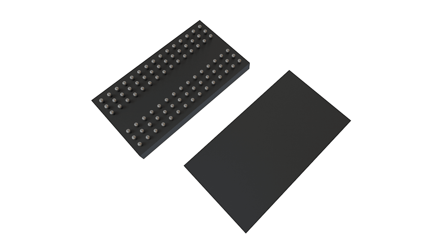
Winbond SDRAM DDR2 W9712G6KB25I, 128 MB, Superficie, TFBGA 16 bit, 84 pines
- Código RS:
- 188-2730
- Nº ref. fabric.:
- W9712G6KB25I
- Fabricante:
- Winbond

Descuento aplicable por cantidad
Ver precios por cantidadSubtotal (1 paquete de 5 unidades)*
11,16 €
(exc. IVA)
13,505 €
(inc.IVA)
Entrega GRATUITA para pedidos superiores a 95,00 €
Agotado temporalmente
- Envío desde el 23 de noviembre de 2026
¿Necesitas comprar más? Introduce la nueva cantidad y clica en "Consultar fechas de entrega"
Unidad(es) | Por unidad | Por Paquete* |
|---|---|---|
| 5 - 5 | 2,232 € | 11,16 € |
| 10 - 15 | 2,03 € | 10,15 € |
| 20 - 45 | 1,992 € | 9,96 € |
| 50 - 95 | 1,968 € | 9,84 € |
| 100 + | 1,766 € | 8,83 € |
*precio indicativo
- Código RS:
- 188-2730
- Nº ref. fabric.:
- W9712G6KB25I
- Fabricante:
- Winbond
Especificaciones
Documentación Técnica
Legislación y Conformidad
Datos del Producto
Encuentra productos similares seleccionando uno o varios atributos.
Seleccionar todo | Atributo | Valor |
|---|---|---|
| Marca | Winbond | |
| Tamaño de la memoria | 128MB | |
| Tipo de producto | SDRAM DDR2 | |
| Organización | 16M x 8 bits | |
| Ancho del bus de datos | 16bit | |
| Número de líneas de bus | 15bit | |
| Número de bits por palabra | 8 | |
| Tiempo de acceso aleatorio máximo | 0.4ns | |
| Número de palabras | 16M | |
| Tipo de montaje | Superficie | |
| Encapsulado | TFBGA | |
| Temperatura de Funcionamiento Mínima | -40°C | |
| Número de pines | 84 | |
| Temperatura de funcionamiento máxima | 95°C | |
| Anchura | 8.1mm | |
| Serie | W9712G6KB | |
| Certificaciones y estándares | RoHS | |
| Longitud | 12.6mm | |
| Altura | 0.8mm | |
| Corriente de suministro | 135mA | |
| Tensión de alimentación máxima | 1.9V | |
| Tensión de alimentación mínima | 1.7V | |
| Estándar de automoción | No | |
| Seleccionar todo | ||
|---|---|---|
Marca Winbond | ||
Tamaño de la memoria 128MB | ||
Tipo de producto SDRAM DDR2 | ||
Organización 16M x 8 bits | ||
Ancho del bus de datos 16bit | ||
Número de líneas de bus 15bit | ||
Número de bits por palabra 8 | ||
Tiempo de acceso aleatorio máximo 0.4ns | ||
Número de palabras 16M | ||
Tipo de montaje Superficie | ||
Encapsulado TFBGA | ||
Temperatura de Funcionamiento Mínima -40°C | ||
Número de pines 84 | ||
Temperatura de funcionamiento máxima 95°C | ||
Anchura 8.1mm | ||
Serie W9712G6KB | ||
Certificaciones y estándares RoHS | ||
Longitud 12.6mm | ||
Altura 0.8mm | ||
Corriente de suministro 135mA | ||
Tensión de alimentación máxima 1.9V | ||
Tensión de alimentación mínima 1.7V | ||
Estándar de automoción No | ||
The W9712G6KB is a 128M bits DDR2 SDRAM and speed involving -25, 25I and -3.
Double Data Rate architecture: two data transfers per clock cycle
CAS Latency: 3, 4, 5 and 6
Burst Length: 4 and 8
Bi-directional, differential data strobes (DQS and /DQS ) are transmitted / received with data
Edge-aligned with Read data and center-aligned with Write data
DLL aligns DQ and DQS transitions with clock
Differential clock inputs (CLK and /CLK)
Data masks (DM) for write data
Commands entered on each positive CLK edge, data and data mask are referenced to both edges of /DQS
Posted /CAS programmable additive latency supported to make command and data bus efficiency
Read Latency = Additive Latency plus CAS Latency (RL = AL + CL)
Off-Chip-Driver impedance adjustment (OCD) and On-Die-Termination (ODT) for better signal quality
Auto-precharge operation for read and write bursts
Auto Refresh and Self Refresh modes
Precharged Power Down and Active Power Down
Write Data Mask
Write Latency = Read Latency - 1 (WL = RL - 1)
Interface: SSTL_18
Enlaces relacionados
- Winbond SDRAM DDR2 Superficie 84 pines
- Winbond SDRAM Superficie 84 pines
- Winbond SDRAM W9751G6NB25I Superficie 84 pines
- Winbond SDRAM Superficie 54 pines
- Winbond SDRAM W9812G6KH-6I Superficie 54 pines
- Winbond SDRAM Superficie 16 bit, 84 pines
- Memoria DDR2 SDRAM W9725G6KB-25/TRAY 800MHZ WBGA, 84 pines DDR2
- Winbond SDRAM W971GG6NB25I Superficie 16 bit, 84 pines